


When we need a microscopic image of our sample, which technique should we use? We could use light, X-rays, electrons, neutrons, atomic force, or tactile sensors as the probe or light source. Different imaging probes and techniques have pros and cons. Of the many imaging techniques, X-ray micro-CT (computed tomography) and SEM (scanning electron microscopy) are among the most widely used techniques for scientific research. Both techniques have advantages and disadvantages.
So, CT or SEM: Which is better? The answer depends on the sample and your research aim. I use X-ray CT every day and am familiar with what it can and can’t do, but I am not an expert on SEM. So, to answer this question for different cases, I invited an SEM expert, Dr. Avery Green from Covalent Metrology. Avery and I answer commonly asked questions about X-ray CT and SEM in this article, and we choose a “winner” for each case.

Guest Expert: Dr. Avery Green, Senior Manager, FIB-SEM | Covalent Metrology
Connect with Avery
Before we dive in, here is a summary of the two techniques:
|
X-ray CT |
SEM |
|
|
Probe |
X-rays |
Electron beam |
|
Dimension |
3D |
2D |
|
Destructive |
No |
No |
|
Resolution |
Submicron - submillimeter |
nm - mm |
|
Environment |
Air |
Vacuum |
|
Sample size |
A few mm - m |
Up to 6” |
|
Material limitation |
Not suitable for materials with no density contrast or high-density materials |
Does not work for liquids, can be destructive with biological samples or soft polymers |
Read: What is micro-CT?
We wanted this article to be comprehensive, but we realize that it’s long. Please feel free to jump to the topic you are interested in.
- Can you do elemental analysis?
- How high is the spatial resolution?
- How big of a sample can you scan?
- Is it destructive?
- What does sample preparation involve?
- Can you see internal structures?
- How long does a measurement take?
- Can you measure my material?
- Can you map crystallinity and crystal orientations?
- When do I need both CT and SEM?
1. Can you do elemental analysis?
Aya: No, unfortunately. Standard laboratory CT doesn’t provide elemental information, although some research examples demonstrate CT elemental analysis (laboratory CT, synchrotron CT examples).
Most commercial CT scanners use absorption contrast imaging and provide relative densities expressed as different gray levels in a CT image. This means that CT is only mapping the density, not elemental composition. However, CT can provide some information about different materials. If you have a standard material that can provide a reference gray level, you can use that to identify materials. Or, if the sample is a mixture of a few known materials, you can identify them easily. Suppose you know your sample is a mixture of glass and polymer. In that case, you can label the bright voxels as “glass” and dark voxels as “polymer,” but that’s as far as CT goes.
Avery: Yes - there are multiple ways that SEM can do elemental analysis. Much like CT, SEM is capable of producing images where grayscale levels show material density (and contrasting areas show differences in density!). This analysis is usually conducted with a backscatter electron (BSE) detector, due to the higher backscatter efficiencies of dense materials relative to light materials. With prior knowledge of sample construction, one can easily identify, for example, tungsten on a silicon background, gold flecks in a carbonaceous powder, or molybdenum inclusions in stainless steel.
SEM can also provide direct information on specific elemental composition with EDS (electron X-ray dispersive spectroscopy) detectors. When high-energy electrons hit a sample, the electrons near its atomic core levels can be knocked out, which allows outer electrons to relax toward the core, and those emit X-rays characteristic of the relaxation energies. This can be thought of as an inverse photoelectric effect. In systems equipped with EDS, the energies of those X-rays are detectable, and the X-ray energy spectrum correlates with the sample’s elemental composition. Modern systems are able to simultaneously make use of the SEM’s ability to generate a beam-rastered image, and the EDS detector’s ability to gather characteristic X-rays, to make compositional maps like the one shown below, which displays the different materials stacked in a nickel-based battery system.
.jpg?width=450&name=SEM%20EDS%20(1).jpg)
Conclusion: SEM-EDS is better.
2. How high is the spatial resolution?
Aya: The sweet spot for CT is in the micron range, where we can use X-ray beam divergence to magnify images. This geometry is called cone beam geometry. It is affordable and widely used for micro-CT.
Laboratory high-resolution CT scanners can achieve submicron spatial resolution by converting X-rays into visible light with a scintillator and magnifying the image using an optical lens. At submicron resolution, you can image things like thin walls of foams and micron-sized fibers in composites in 3D and perform quantitative analysis, as shown in the examples below.
.jpg?width=450&name=XCT%20foam%20composite%20application%20insulator%203-min%20(1).jpg)
Wall thickness analysis of a heat insulator (Minimum cell wall thickness ~ 1 micron)
.jpg?width=600&name=XCT%20foam%20and%20composite%20application%20CFRP%20video%204-min%20(1).jpg)
CFRP (carbon fiber reinforced polymer) fiber orientation analysis (Carbon fiber diameter ~ 7.5 microns)
A few ultrahigh-resolution CT scanners and synchrotron beamlines can reach about 20-50 nm by using Fresnel zone plates or multilayer mirrors to function as lenses. These experimental setups are somewhat specialized, meaning they are less versatile and accessible.
Despite the short wavelength of X-rays, X-ray CT resolution is limited because we can’t make efficient lenses for X-rays. I’d recommend SEM or TEM (transmission electron microscopy) for nanometer-scale imaging.
Read: “How to improve the resolution of X-ray CT images”
Avery: Resolution is a strong point for SEM. Most modern systems have “information limits” that are sub-nanometer but, in practice, you can usually resolve features pretty well down to about 10 nanometers and, after that, features become blurry. Traditional SEMs usually rely on high-accelerating energies and low working distances to create a sharp beam and to resolve the smallest features–and to be sure, this is still a useful strategy for a lot of samples. But not all samples are created equal. We often see, for example, highly electrically insulating samples. Modern advances with beam energy filtering, detector energy filtering, magnetic field immersion, and beam deceleration have pushed high-resolution imaging outside the purview of high-energy experiments. These advances have allowed low-landing energy imaging to achieve UHR (ultrahigh-resolution) imaging capabilities.
.jpg?width=450&name=hihg-resolution%20SEM%20(1).jpg)
Conclusion: SEM is better for nanometer resolution. CT can work submicron to micron resolution.
3. How big of a sample can you scan?
Aya: You can scan 1~2 m tall samples with large-scale high-energy industrial CT scanners, but there are a few things to keep in mind. The denser and thicker the sample is, the higher the required X-ray energy to get through the sample. This means not only that you need a large CT scanner, but you also need a high-energy (200 - 400 kV applied voltage) X-ray source. These CT scanners can cost close to or over $1M, while a benchtop scanner that can scan something like a smartphone costs less than $300K.
Another thing to note about scanning large samples is that the resolution decreases as the scanned area size (FOV: field of view) becomes larger. The voxel resolution is roughly 1/1000 to 1/3000 of the scanned area size. (Note: The spatial resolution is about double the voxel resolution.)
Here are examples of different sample sizes, FOVs, and voxel resolution. As you see on the left, to scan a foam material with 0.325 microns/voxel resolution, realistically, you want to set the FOV to 0.5 - 1 mm. To scan a shark tooth, you want to set the FOV to about 25 mm, which provides 5-10 microns/voxel resolution. Then to scan an entire smartphone, the FOV needs to be about 200 mm. In that case, the voxel resolution is 30-100 microns.
.jpg?width=600&name=CT-FOV%20and%20voxel%20resolution-min%20(1).jpg)
Avery: SEMs come in a large variety of sizes but, in general, are built to handle samples under 6” in diameter. Typical samples are on the order of 1” across, and there are not any samples that are too small to be measured. Large samples, however, can become a problem. Because SEMs operate under high vacuum, they are uniformly designed as closed chambers with rigid walls that cannot easily be modified to accommodate large samples. There are some exceptions–semiconductor wafer fabrication plants have SEMs that can accommodate 12” samples (that are exactly circular and about 0.8 mm thick with little tolerance), and USAF has an SEM with a chamber size of over 300 cubic feet! Typical lab-scale SEMs do quite well with samples on the order of 1” and usually have 5-axis stage control (X, Y, Z, rotation, and tilt), which can ensure that small features can be found and oriented for specific imaging requests.
Conclusion: CT can scan larger samples than SEM.
4. Is it destructive?
Aya: No, CT is a non-destructive 3D imaging technique. Commercial CT scanners were first developed to scan human brains. If your doctor is going to scan your brain, you would hope it is non-destructive. You don’t need to section, dry, or coat the sample. Even soft tissues and live plants can be scanned without any significant damage. The ability to scan the entire volume of an object non-destructively is one of the most significant advantages of this technique.
Because CT is non-destructive, it is also used to image valuable objects such as archeological samples and fossils.
.jpg?width=600&name=XCT%20geology%20application%20amonite%202-min%20(1).jpg)
CT scan of an ammonite fossil (Perisphinctes). CT cross-section (left) and extracted surface mesh (right).
Avery: This question can be a little complicated for SEMs, and even more so for FIB-SEMs. For most inorganic materials, neither the vacuum chamber nor the electron beam cause any damage. Organic samples, on the other hand, can be much more delicate. When hit with an electron beam, they often (1) capture electrons and charge up, (2) heat up to near their melting temperature, or (3) shrink, shrivel, or cure into different surface shapes. Typically, you will coat those soft organic materials with a thin metal layer to dissipate heat and charge, and no significant damage is done during imaging. As long as samples are properly prepared, SEM is generally a non-destructive technique.
Many SEMs have a focused ion beam (FIB) in addition to the electron beam (and are colloquially referred to as dual-beam systems). These FIBs often contain gallium, which is ~125,000 times heavier than an electron and readily sputters away the sample surface. This can be a very helpful feature, and is often used to dig microscopic holes near the surface of a sample. The microscopic holes can be imaged as cross-sections! While this process is technically destructive, it’s purposeful, and the destruction is usually on a scale too small to see with the human eye. The image below was generated by cutting a cross-section into a sample surface and imaging the vertical face of that cut.
.jpg?width=450&name=FIB%20cross%20sectional%20SEM%20(1).jpg)
Conclusion: Both techniques are non-destructive for most inorganic materials. CT is better for organic materials.
5. What does sample preparation involve?
Aya: Sample preparation for X-ray CT is next to none. Most samples can be scanned as is because the sample can sit in the air and does not require conductivity. Samples can be wet or even kept in a solution. Below is a CT scan of live tomato plant roots..jpg?width=350&name=tomato%20roots%20(1).jpg) The exceptions are life science samples such as organ tissues, insects, etc. These samples often need to be fixed for preservation and also stained to enhance the contrast between tissues with very similar X-ray absorption coefficients.
The exceptions are life science samples such as organ tissues, insects, etc. These samples often need to be fixed for preservation and also stained to enhance the contrast between tissues with very similar X-ray absorption coefficients.
One thing that can be tricky is the sample mount. When running a high-resolution scan, you need to make sure the sample doesn’t move or change its shape and size. If the sample moves 1 micron during a submicron resolution scan, the resulting CT image would be blurred. If a wet sample dries up and shrinks during a scan, that can also blur the CT image. In this case, you can coat or seal the sample to prevent it from drying.
Avery: Some preparation is needed for most samples in SEM. Small samples have relevant features directly on the surface, and are electrically conductive–these can often be adhered to a stub and put into the SEM chamber. As mentioned above, not all samples are created equal. We see samples ranging from liquid suspensions, magnetic powders, patterned ICs, glass capillaries, thinly coated diamond, battery electrodes, etc. With the right tool and preparation method, they can be measured. Common SEM preparation methods include globally depositing a thin metal layer, drop-casting liquids and drying in vacuum, and grounding contacts on IC samples.
Conclusion: CT sample preparation is easier.
6. Can you see internal structures?
Aya: Yes! CT can image the entire volume of an object non-destructively. A 3D CT image consists of multiple, often hundreds to thousands of, cross-sections. Once you obtain a CT scan, you can look at a cross-section of the sample at whatever position or angle you like without sectioning the sample.
You can see the internal structures because we use X-ray transmission images, also called 2D projections or radiographs. A radiograph is a map of X-ray intensity transmitted through the sample. It contains information related to the absorption coefficient distribution of the sample, including the internal structures. One radiograph has all the structures projected onto one plane and does not provide three-dimensional information. But by collecting hundreds to thousands of radiographs from different angles, we can reconstruct the 3D density distribution.
Here is an example of a broken wire bonding inside an LED chip. You can see this type of defect without opening the package or damaging the device.
.jpg?width=350&name=XCT%20misc%20application%20LED-3-min%20(1).jpg)
Avery: With a single-beam SEM, you can only see the surface. Unlike X-rays, electrons cannot transmit through materials (except in the case of high-energy electrons and very thin materials, as in TEM), and the signal is purely generated by the interaction between the electron beam and the sample surface. That said, dual-beam FIB-SEMs can be equipped to see inside samples. The method used to see “inside” samples with FIB-SEM is called FIB-SEM tomography, which we do using a program called Thermo Fisher Slice and View. This method uses both the FIB’s cutting capability and any common imaging technique (SEM, EDS, EBSD), and alternates between those functions to take data at small slices until a full 3D volume of data has been collected. The figure below shows one image acquired during a FIB tomography experiment, and a 3D model generated from one of the material types shown in the boxed area.
.jpg?width=602&name=FIB%20SEM%203D%20(1).jpg)
Conclusion: CT can see internal structure non-destructively. FIB-SEM can see internal structure by cutting into the sample.
7. How long does a measurement take?
Aya: It depends. A typical CT scan time is about 30 minutes to a few hours. However, depending on the required image quality, mainly the resolution and signal-to-noise ratio, it can vary from a few seconds to tens of hours. The scan time increases as you try to increase the resolution or reduce the noise level. When you conduct an in-situ experiment or time-resolved CT (4DCT), the scan time might need to be short.
For example, suppose you want to check if there are broken circuits in a PCB board. In that case, a 5-minute scan might suffice. But suppose you were to quantify the fiber orientation distribution of 7-micron carbon fibers in CFRP parts. In that case, you might need a 5-hour scan.
For 4DCT, the scan time often needs to be short. Here is an example. We collected each image in 18 seconds at 72 mm FOV and 144 micron/voxel resolution to see a bread dough rise.
.jpg?width=700&name=bread%20dough%20CT%20scans-min%20(1).jpg)
Here is an example of a slow high-resolution scan. To achieve 0.26 micron/voxel resolution using a CCD detector, we set the FOV to 0.7 mm and ran a 9.5-hour scan to see the 1-2 microns thick polyurethane cell walls.
.jpg?width=600&name=foam%20CT%20scan-min%20(1).jpg)
Avery: A single SEM image can take as little as 10 seconds to acquire. Nevertheless, that does not consider sample preparation time and does not usually provide sufficient information to answer materials science questions.
A typical set of SEM image data may include images from 100 to 100,000x magnification, detectors for both secondary and backscatter imaging, multiple rotations or tilts to see features with varying perspectives, EDS and/or EBSD data, etc. We usually plan on spending a few hours to characterize a sample’s morphology and composition, although timing can vary significantly.
Conclusion: The purpose of the experiment and required image quality dictate the measurement time in both cases.
8. Can you measure my material?
Aya: For CT, whether or not you can measure a particular material depends on the material’s density and sample thickness. To give you an idea, with a 130 kV X-ray source commonly used in small-to-mid-size micro-CT scanners, you can scan a few tens of millimeters thick aluminum or a few millimeters thick iron. You can scan denser and thicker parts, such as automobile parts, with an over 200 kV source. Even a MV source is now available to scan denser and larger samples.
To obtain a decent CT image, we need some X-ray photons to survive; i.e., get through the sample and generate 2D projections. As a sample becomes denser or thicker, it gets harder for X-rays to survive. Higher-energy X-ray photons have an easier time surviving. The graph below shows how many X-ray photons can “survive” a certain sample by percentage compared to the incident X-ray photon count.
.png?width=600&name=X-ray%20survival%20vs%20source%20energy%20for%20thickness%20(1).png) (Calculated using MuCalc)
(Calculated using MuCalc)
You can see both the material density and thickness matter. At low energy, around 10 keV, virtually no X-ray photons can get through 1 mm thick aluminum. As the energy goes higher, the survival rate goes up. But for 100 mm thick aluminum, only a few percent of X-ray photons can survive the penetration process even at 200 keV.
Finally, note that when you apply 200 kV to the X-ray source, the peak energy is around 100 - 150 keV, depending on the filter. In other words, to have 200 keV peak energy, you need to apply about 400 kV to the X-ray source.
Next, let’s think about light materials. X-ray CT does not require any special sample preparation and is suitable to image wet samples, including soft tissues and plants. These materials and other organic and carbon-based materials are light-absorbing.
To image light materials, you want to use low-energy X-rays to achieve high contrast. As you can see in the graph above, graphite, even at 10 mm thickness, permits the majority of the X-rays above 60 keV. If most of the X-rays go through the sample without being absorbed, you can’t get good contrast in your CT images. Low-energy X-rays are easily absorbed by light materials and create excellent absorption contrast.
Avery: Nearly all SEM experiments are confined to solids. Liquids tend to evaporate in vacuum or when heated by the electron beam.
Aside from that, the main obstacle we face in materials is electrical insulation. Because SEM (and FIB) experiments all rely on the injection of a charged particle beam into the surface, if the charge cannot find a path to ground, it builds up and causes problems. In ideal samples, like metals, the ~0.1 nA electron beam impacts and enters the material surface and can conduct away from the imaging area, leaving the imaging area in a stationary and uncharged state. In samples with insulating materials that cannot have grounding contacts nearby, the electron beam causes charging (see the image below). The charging causes the sample to move around, or causes local areas to start to pool electrons and give off a high-intensity streaky signal. We typically coat insulating materials with an ~10-nanometer layer of metal that connects to a grounded area so that charge can be dissipated. If the sample is meant to be kept in pristine condition, we can use some other tricks, typically involving very low-beam energies and currents, to generate good SEM images from insulating samples.
SEM measurements can be further complicated by “soft” materials, by which we usually mean polymers or biological samples. These carbonaceous materials are not only electrically insulating, but they are often heat-sensitive and less physically robust than metals or semiconductors. When we do SEM on these samples, we often see charging, but with most current levels in a field-emission SEM, no significant damage is done. However, FIB can be disastrous on soft materials if conventional beam conditions are used. Patterned photoresists, for example, often burn, melt, or disintegrate when a 30 kV FIB hits nearby. Fortunately, we can adjust the energy and current of the FIB as well and can often create smooth cuts without damaging soft materials using longer, gentler cutting conditions.
.jpg?width=450&name=SEM%20charge%20problem%20(1).jpg)
Conclusion: CT is more versatile than SEM.
9. Can you map crystallinity and crystal orientations?
Aya: If there is a density difference between the crystalline and amorphous phases, you can map these two phases and calculate crystallinity. It can work on some organic materials. About 5% or greater density difference has a chance of generating enough contrast in organic materials.
Here is an example of pharmaceutical tablets. The crystalline API has an 8% higher density than the amorphous API and the polymer matrix in these tablets. So the crystalline API appeared brighter in the CT image. The crystalline phase is colored yellow in this figure.
.jpg?width=600&name=XCT%20pharma%20application%20crystallinity-unisize-min%20(1).jpg)
Absorption-contrast-based X-ray CT cannot map crystal orientation because all crystallites have the same absorption coefficient. Diffraction-contrast-based X-ray CT can map crystal orientations in 3D. The analysis technique has advanced in recent years, and it is applied to various materials, such as ceramics and metals. (See an example of diffraction contrast imaging by Sya et al. (2012) Scr. Mater., 66(1), 1-4.)
Avery: SEM can measure crystallinity in multiple ways. We can gather information about grain sizes, and if there is extra information available, we may be able to correlate it with specific phase information or orientation. At a less detailed level, SEM and FIB imaging create contrast based on crystal orientations, as shown in the image below.
.jpg?width=500&name=SEM%20crystal%20grains%20(1).jpg)
SEM does have the option of an extra diffraction detector, enabling a technique called electron backscatter diffraction (EBSD). As you might expect from the name, this is a measurement of electrons diffracted from the sample surface, typically done in reflection geometry. We raster the electron beam over the sample and capture a Kikuchi pattern at each pixel in this mode. These patterns contain complete information about the structure and orientation of the crystal lattice detected at each pixel and, with guidance, our software can automatically identify crystal grains. These scans contain a wealth of information about crystallinity and are spatially resolved. With this information, one could measure grain size distribution as a function of position, trends in strain, get degrees of preferred grain orientation, make pole figures, etc.
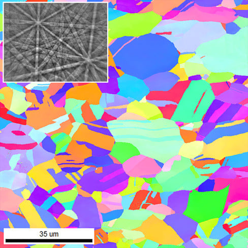
Conclusion: SEM is suitable for crystallinity and crystalline orientation analysis.
10. When do I need both CT and SEM?
Aya: X-ray CT is often used to “scout” a large sample to find a good location to cut out for SEM or other higher-resolution imaging.
When you need a wide range of length scales, you might need both CT and SEM. A typical example is digital rock analysis. Analysis of an entire drill core requires a CT scan. Creating a 3D map of grains in a sandstone, for example, also requires a CT scan. These scans are used to construct a digital rock so that we can calculate permeability, simulate oil and brine flow, etc., without running time-consuming and expensive experiments.
But if the sandstone includes porous materials such as clay, then running simulations based on the micron-sized pores we can see with X-ray CT is inaccurate. We need SEM to obtain a higher-resolution image of the clay to calculate the porosity and permeability of the clay at the nanoscale. By combining both the micro- and nanoscale information, you can simulate various experiments more accurately. (See an example by A. Jacob et al. (2020), Solid Earth, 12, 1–14.)
Avery: The question of which technique to use is mostly a question of scale. CT works wonders for samples with feature sizes above the micron range, and SEM fits well with problems that need nanometer resolution. Many experiments involve starting with large samples and looking for tiny targets. With both techniques, you could start with a PCB with a short identified in electrical data, generate a 3D representation of the part with CT, find an anomalous gap in the insulating layer, take the part to SEM, and image the region of interest to find that there was a conductive nanoparticle in the insulating layer, which caused the short!
Conclusion: When you need to cover a wide range of scale, you need both CT and SEM.
Which technique is right for me?
We hope we answered some of the questions you had about CT and SEM. Remember that this is not a question of whether CT or SEM is better despite the title of the article. These techniques often complement each other. The best way to figure out which technique is right for you is to talk to an expert about your specific samples and research needs.
Both techniques offer unique advantages, and can provide critical data to help understand material structure and phase. With a combination of CT and SEM, you can generate 3D models of materials from the cm scale to the nm scale!
If you are interested in or have questions about CT, our team of Rigaku application scientists can help you. You can talk to one of our CT experts by clicking the “Talk to an expert” button at the right top of the page or send us a message at imaging@rigaku.com.
If you are interested in SEM, Covalent Metrology offers a full suite of S/TEM analytical services, including advanced sample preparation capabilities. For clients wishing to participate in their sample’s analysis, Covalent also offers free Live View services for both Micro-CT and SEM - live analysis sessions with a Covalent Expert. Contact Covalent for a free project consultation today at hello@covalentmetrology.com.